Page 234 - DCAP108_DIGITAL_CIRCUITS_AND_LOGIC_DESIGNS
P. 234
Unit 12: A/D and D/A Converters


            Solution:                                                                             Notes
            The LSB of an 11-bit system has a resolution of 1/2048. This would provide a resolution at the
            output of 1/2048 * (+10) = +5 mV.
            It is important to realize that resolution and accuracy in a system should be compatible. For
            example, in the 4-bit system previously discussed, the resolution was found to be 1 V. Clearly it
            would be unjustifiable to construct such a system to an accuracy of 0. 1%. This would mean that the
            system would be accurate to 16 mV but would be capable of distinguishing only to the nearest 1 V.
            Similarly, it would be wasteful to construct the 11-bit system described in Example 12.11 to an
            accuracy of only 1 percent. This would mean that the output voltage would be accurate only to
            100 mV, whereas it is capable of distinguishing to the nearest 5 mV.

            12.5 A/D Converter—Simultaneous Conversion


            The process of converting an analog voltage into an equivalent digital signal is known as analog-
            to-digital (A/D) conversion. This operation is somewhat more complicated than the converse
            operation of D/A conversion. A number of different methods have been developed, the simplest
            of which is probably the simultaneous method.

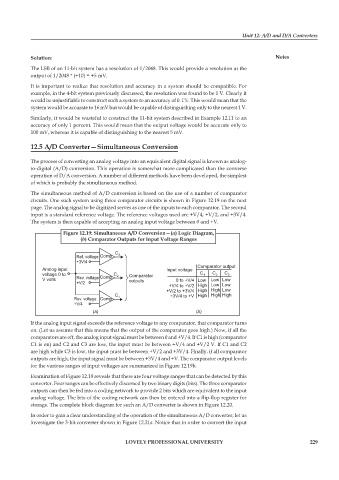
            The simultaneous method of A/D conversion is based on the use of a number of comparator
            circuits. One such system using three comparator circuits is shown in Figure 12.19 on the next
            page. The analog signal to be digitized serves as one of the inputs to each comparator. The second
            input is a standard reference voltage. The reference voltages used are +V/4, +V/2, and +3V/4.
            The system is then capable of accepting an analog input voltage between 0 and +V.
                       Figure 12.19: Simultaneous A/D Conversion—(a) Logic Diagram,
                             (b) Comparator Outputs for Input Voltage Ranges

                                         C
                            Ref. voltage Comp.  3
                            +3V/4
                                                                      Comparator output
                Analog input                                Input voltage
                voltage0to               C 2  Comparator               C 1  C 2  C 3
                V volts     Rev. voltage Comp.  outputs        0to +V/4 Low  Low Low
                            +V/2
                                                            +V/4 to +V/2 High Low Low
                                                           +V/2 to +3V/4 High High Low
                                         C                   +3V/4 to +V High High High
                           Rev. voltage Comp.  1
                           +V/4
                                                                      b
                                  a
                                  ()                                  ()
            If the analog input signal exceeds the reference voltage to any comparator, that comparator turns
            on. (Let us assume that this means that the output of the comparator goes high.) Now, if all the
            comparators are off, the analog input signal must be between 0 and +V/4. If C1 is high (comparator
            C1 is on) and C2 and C3 are low, the input must be between +V/4 and +V/2 V. If C1 and C2
            are high while C3 is low, the input must be between +V/2 and +3V/4. Finally, if all comparator
            outputs are high, the input signal must be between +3V/4 and +V. The comparator output levels
            for the various ranges of input voltages are summarized in Figure 12.19b.

            Examination of Figure 12.19 reveals that there are four voltage ranges that can be detected by this
            converter. Four ranges can be effectively discerned by two binary digits (bits). The three comparator
            outputs can then be fed into a coding network to provide 2 bits which are equivalent to the input
            analog voltage. The bits of the coding network can then be entered into a flip-flop register for
            storage. The complete block diagram for such an A/D converter is shown in Figure 12.20.
            In order to gain a clear understanding of the operation of the simultaneous A/D converter, let us
            investigate the 3-bit converter shown in Figure 12.21a. Notice that in order to convert the input


                                             LOVELY PROFESSIONAL UNIVERSITY                                   229

