Page 219 - DCAP108_DIGITAL_CIRCUITS_AND_LOGIC_DESIGNS
P. 219
Digital Circuits and Logic Design


                   Notes                       12.1: Find the binary equivalent weight of each bit in a 4-bit system.

                                 Solution:
                                 LSB has a weight of 1/(2  – 1) = 1/(16 – 1) = 1/15, or 1 part in 15. The second LSB has a weight
                                                     4
                                 of 2 *1/15 = 2/15. The third LSB has a weight of 4 *1/15 = 4/15 and the MSB has a weight of 8
                                 *1/15 = 8/15. As a check, the sum of the weights must equal 1. Thus 1/15 + 2/15 + 4/15 + 8/15 =
                                 15/15 = 1. The binary equivalent weights for 3-bit and 4-bit system are summarized in Figure 12.2.

                                                Always remember to divide the analog signal into seven levels, in binary
                                                equivalent weight.
                                 12.1.2 Resistive Divider

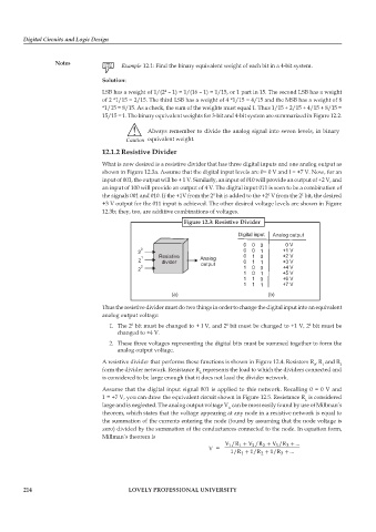
                                 What is now desired is a resistive divider that has three digital inputs and one analog output as
                                 shown in Figure 12.3a. Assume that the digital input levels are 0= 0 V and l = +7 V. Now, for an
                                 input of 001, the output will be + 1 V. Similarly, an input of 010 will provide an output of +2 V, and
                                 an input of 100 will provide an output of 4 V. The digital input 011 is seen to be a combination of
                                 the signals 001 and 010. If the +1V from the 2  bit is added to the +2  V from the 2  bit, the desired
                                                                     0
                                                                                      0
                                                                                                 1
                                 +3 V output for the 011 input is achieved. The other desired voltage levels are shown in Figure
                                 12.3b; they, too, are additive combinations of voltages.
                                                           Figure 12.3: Resistive Divider


                                 Thus the resistive divider must do two things in order to change the digital input into an equivalent
                                 analog output voltage:
                                    1.  The 2  bit must be changed to + l V, and 2  bit must be changed to +1 V, 2  bit must be
                                                                         1
                                           0
                                                                                                   2
                                      changed to +4 V.
                                    2.  These three voltages representing the digital bits must be summed together to form the
                                      analog output voltage.
                                 A resistive divider that performs these functions is shown in Figure 12.4. Resistors R , R  and R
                                                                                                    0  1     2
                                 form the divider network. Resistance R  represents the load to which the dividers connected and
                                                                L
                                 is considered to be large enough that it does not load the divider network.
                                 Assume that the digital input signal 001 is applied to this network. Recalling 0 = 0 V and
                                 1 = +7 V, you can draw the equivalent circuit shown in Figure 12.5. Resistance R  is considered
                                                                                                  L
                                 large and is neglected. The analog output voltage V  can be most easily found by use of Millman’s
                                                                         A
                                 theorem, which states that the voltage appearing at any node in a resistive network is equal to
                                 the summation of the currents entering the node (found by assuming that the node voltage is
                                 zero) divided by the summation of the conductances connected to the node. In equation form,
                                 Millman’s theorem is
                                                                        V / R +  V / R +  V / R + ...
                                                                   V  =   1  1   2  2   3   3
                                                                          1/ R +  1  1/ R +  2  1/ R + ...
                                                                                          3


        214                               LOVELY PROFESSIONAL UNIVERSITY

