Page 223 - DCAP108_DIGITAL_CIRCUITS_AND_LOGIC_DESIGNS
P. 223

Digital Circuits and Logic Design


                   Notes
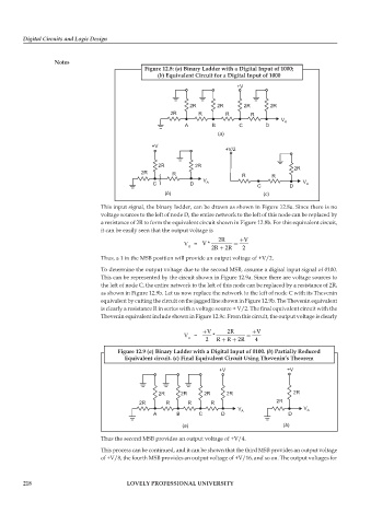
                                               Figure 12.8: (a) Binary Ladder with a Digital Input of 1000;
                                                    (b) Equivalent Circuit for a Digital Input of 1000

                                                                             +V


                                                              2R       2R      2R       2R
                                                        2R       R       R        R
                                                                                           V A
                                                            A        B        C       D
                                                                       a
                                                                       ()
                                                  +V
                                                                         +V/2

                                                    2R          2R
                                                                                               2R
                                              2R        R                      R        R
                                                                  V                               V
                                                  C           D    A                               A
                                                                                    C         D
                                                      ()                              ()
                                                      b
                                                                                      c
                                 This input signal, the binary ladder, can be drawn as shown in Figure 12.8a. Since there is no
                                 voltage sources to the left of node D, the entire network to the left of this node can be replaced by
                                 a resistance of 2R to form the equivalent circuit shown in Figure 12.8b. For this equivalent circuit,
                                 it can be easily seen that the output voltage is
                                                                       2 R    + V
                                                            V   =  V *  2 R +  2 R  =  2
                                                             A
                                 Thus, a 1 in the MSB position will provide an output voltage of +V/2.
                                 To determine the output voltage due to the second MSB, assume a digital input signal of 0100.
                                 This can be represented by the circuit shown in Figure 12.9a. Since there are voltage sources to
                                 the left of node C, the entire network to the left of this node can be replaced by a resistance of 2R,
                                 as shown in Figure 12.9b. Let us now replace the network to the left of node C with its Thevenin
                                 equivalent by cutting the circuit on the jagged line shown in Figure 12.9b. The Thevenin equivalent
                                 is clearly a resistance R in series with a voltage source + V/2. The final equivalent circuit with the
                                 Thevenin equivalent include shown in Figure 12.9c. From this circuit, the output voltage is clearly

                                                                  +V      2 R     +V
                                                            V   =   2  *  R  + R  + R  =  4
                                                             A
                                                                             2
                                       Figure 12.9 (a) Binary Ladder with a Digital Input of 0100. (b) Partially Reduced
                                         Equivalent circuit. (c) Final Equivalent Circuit Using Thevenin’s Theorem

                                                                       +V                    +V


                                                    2R     2R      2R     2R                   2R
                                              2R      R      R       R                    2R
                                                                             V                     V A
                                                  A       B      C      D     A               D
                                                                                            b
                                                            ()                              ()
                                                            a
                                 Thus the second MSB provides an output voltage of +V/4.
                                 This process can be continued, and it can be shown that the third MSB provides an output voltage
                                 of +V/8, the fourth MSB provides an output voltage of +V/16, and so on. The output voltages for


        218                               LOVELY PROFESSIONAL UNIVERSITY
   218   219   220   221   222   223   224   225   226   227   228