Page 29 - DCAP108_DIGITAL_CIRCUITS_AND_LOGIC_DESIGNS
P. 29
Digital Circuits and Logic Design


                   Notes         2.1.4 NAND Gate
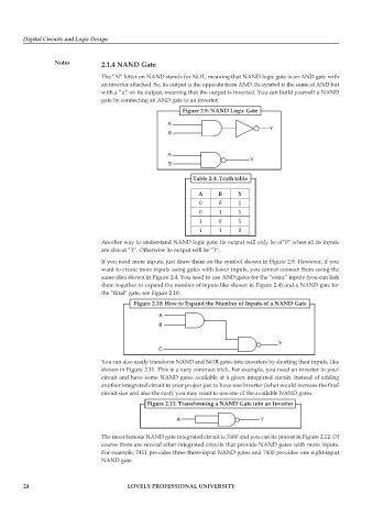
                                 The ”N“ letter on NAND stands for NOT, meaning that NAND logic gate is an AND gate with
                                 an inverter attached. So, its output is the opposite from AND. Its symbol is the same of AND but
                                 with a ”o“ on its output, meaning that the output is inverted. You can build yourself a NAND
                                 gate by connecting an AND gate to an inverter.
                                                           Figure 2.9: NAND Logic Gate


                                                               Table 2.4: Truth table

                                                                A      B     Y
                                                                 0     0     1
                                                                 0     1     1
                                                                 1     0     1
                                                                 1     1     0

                                 Another way to understand NAND logic gate: its output will only be at”0“ when all its inputs
                                 are also at ”1“. Otherwise its output will be ”1“.
                                 If you need more inputs, just draw them on the symbol shown in Figure 2.9. However, if you
                                 want to create more inputs using gates with fewer inputs, you cannot connect them using the
                                 same idea shown in Figure 2.4. You need to use AND gates for the “extra” inputs (you can link
                                 them together to expand the number of inputs like shown in Figure 2.4) and a NAND gate for
                                 the ”final“ gate, see Figure 2.10.
                                            Figure 2.10: How to Expand the Number of Inputs of a NAND Gate


                                 You can also easily transform NAND and NOR gates into inverters by shorting their inputs, like
                                 shown in Figure 2.11. This is a very common trick. For example, you need an inverter in your
                                 circuit and have some NAND gates available at a given integrated circuit. Instead of adding
                                 another integrated circuit to your project just to have one inverter (what would increase the final
                                 circuit size and also the cost), you may want to use one of the available NAND gates.
                                                Figure 2.11: Transforming a NAND Gate into an Inverter


                                 The most famous NAND gate integrated circuit is 7400 and you can its pinout in Figure 2.12. Of
                                 course there are several other integrated circuits that provide NAND gates with more inputs.
                                 For example, 7411 provides three three-input NAND gates and 7430 provides one eight-input
                                 NAND gate.


        24                                LOVELY PROFESSIONAL UNIVERSITY

