Page 54 - DCAP108_DIGITAL_CIRCUITS_AND_LOGIC_DESIGNS
P. 54
Unit 3: Boolean Algebra


                                                                                                  Notes
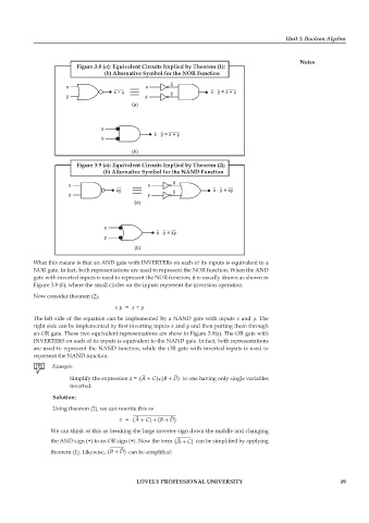
                          Figure.3.8 (a): Equivalent Circuits Implied by Theorem (1):
                                 (b) Alternative Symbol for the NOR Function

                                                        x
                      x                         x
                                      x+y               y            x . y=x+y
                      y                         y
                                            a
                                            ()


                                  x
                                                   x . y=x+y
                                  y
                                            ()
                                            b
                          Figure 3.9 (a): Equivalent Circuits Implied by Theorem (2);
                                (b) Alternative Symbol for the NAND Function
                                                         x
                       x                         x
                                       xy                y            x . y=xy
                       y                         y
                                            ()
                                             a


                                   x
                                                    x . y=xy
                                   y

                                            ()
                                             b
            What this means is that an AND gate with INVERTERs on each of its inputs is equivalent to a
            NOR gate. In fact, both representations are used to represent the NOR function. When the AND
            gate with inverted inputs is used to represent the NOR function, it is usually drawn as shown in
            Figure 3.8 (b), where the small circles on the inputs represent the inversion operation.

            Now consider theorem (2),
                                      x y  =  x + y
            The left side of the equation can be implemented by a NAND gate with inputs x and y. The
            right side can be implemented by first inverting inputs x and y and then putting them through
            an OR gate. These two equivalent representations are show in Figure 3.9(a). The OR gate with
            INVERTERS on each of its inputs is equivalent to the NAND gate. In fact, both representations
            are used to represent the NAND function, while the OR gate with inverted inputs is used to
            represent the NAND function.


                        Simplify the expression z =  (A + C ) (B +  D )  to one having only single variables
                                                    •
                        inverted.
                  Solution:
                  Using theorem (2), we can rewrite this as

                                        z  =  (A +  C ) +  (B +  D )
                 We can think of this as breaking the large inverter sign down the middle and changing
                 the AND sign (•) to an OR sign (+). Now the term  (A + C )  can be simplified by applying
                 theorem (1). Likewise,  (B + D )  can be simplified:


                                             LOVELY PROFESSIONAL UNIVERSITY                                    49

