Page 104 - DCAP210_INTRODUCTION__TO_MICROPROCESSORS
P. 104
Introduction to Microprocessors


                  Notes          Introduction

                                 While executing a program, the microprocessor needs to access memory frequently to read
                                 instruction codes and data stored in memory and the interfacing circuit enables that access.
                                 Memory is basically a data storage device. For any microprocessor system we require memories
                                 to store monitor program, to store data. So memory is an essential component in microprocessor
                                 system which will allow the user to store the program and data. Memory consists of thousand of
                                 memory cells is capable of storing 1-bit.

                                 7.1 Memory Structure and its Requirements
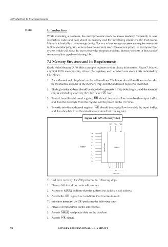
                                 Read/Write Memory (R/WM) is a group of registers to store binary information. Figure 7.1 shows
                                 a typical R/W memory chip, it has 1024 registers, each of which can store 8 bits indicated by
                                 8 I/O lines.

                                 1. An address should be placed on the address lines. The low-order address lines are decoded
                                    by the internal decoder of the memory chip, and the addressed register is identified.

                                 2. The high-order address should be decoded to generate a Chip Select signal, and the memory
                                    chip is selected by asserting the Chip Select  CS  low.
                                 3. To read from the addressed register,  RD  should be asserted low to enable the output buffer,
                                    and then the data byte from the register will be placed on the I/O lines.
                                 4. To write into the addressed register,  WR  should be asserted low to enable the input buffer,
                                    and then data bits from the data lines are stored into the register.

                                                           Figure 7.1: R/W Memory Chip


                                 To read from memory, the Z80 performs the following steps:
                                 1. Places a 16 bit address on its address bus.

                                 2. Asserts to  MREQ  indicate that the address bus holds a valid address.
                                 3. Asserts the  RD  signal low to indicate that it wants to read.
                                 To write into memory, the Z80 performs the following steps:

                                 1. Places a 16 bit address on the address bus.
                                 2. Asserts  MREQ  and places data on the data bus.
                                 3. Asserts  WR  signal.


        98                               LOVELY PROFESSIONAL UNIVERSITY

