Page 173 - DCAP403_Operating System
P. 173
Operating System


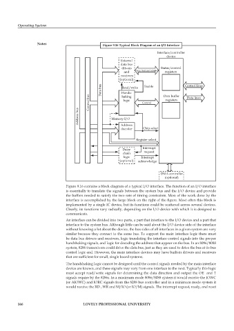
                    Notes                            Figure 9.16 Typical Block Diagram of an I/O Interface

                                                                                 Interface/controller
                                                                                      device
                                                              External
                                                              data bus
                                                               drivers             Status/control
                                                                and   Data/status/control  registers
                                                               receivers
                                                              (optional)
                                                    Data bus   Hands-     Enable    Data buffer  Control lines
                                                               Read/write
                                              Control bus      haking    Control     registers  Data lines
                                                                logic

                                         Address bus      Memory-I/O


                                                              Address
                                                               decoder    Chip select


                                                                      Register select

                                                               Daisy      Interrupt
                                                                chain     request
                                                                logic    Interrupt
                                                              (optional)  acknowledge


                                                                                   DMA controller
                                                                                     (optional)
                                   Figure 9.16 contains a block diagram of a typical I/O interface. The function of an I/O interface
                                   is essentially to translate the signals between the system bus and the I/O device and provide
                                   the buffers needed to satisfy the two sets of timing constraints. Most of the work done by the
                                   interface is accomplished by the large block on the right of the figure. Most often this block is

                                   implemented by a single IC device, but its functions could be scattered across several devices.
                                   Clearly, its functions vary radically, depending on the I/O device with which it is designed to
                                   communicate.
                                   An interface can be divided into two parts, a part that interface to the I/O device and a part that
                                   interface to the system bus. Although little can be said about the I/O device side of the interface
                                   without knowing a lot about the device, the bus sides of all interfaces in a given system are very
                                   similar because they connect to the same bus. To support the main interface logic there must
                                   be data bus drivers and receivers, logic translating the interface control signals into the proper
                                   handshaking signals, and logic for decoding the address that appear on the bus. In an 8086/8088
                                   system, 8286 transceivers could drive the data bus, just as they are used to drive the bus at its bus
                                   control logic end. However, the main interface devices may have built-in drivers and receivers

                                   that are sufficient for small, single board systems.
                                   The handshaking logic cannot be designed until the control signals needed by the main interface
                                   device are known, and these signals may vary from one interface to the next. Typically this logic
                                   must accept read/write signals for determining the data direction and output the OE  and T
                                   signals require by the 8286s. In a maximum mode 8086/8088 system it would receive the IOWC
                                   (or AIOWC) and IORC signals from the 8288 bus controller and in a minimum mode system it
                                   would receive the RD , WR and M/IO (or IO/M) signals. The interrupt request, ready, and reset


          166                              LOVELY PROFESSIONAL UNIVERSITY

