Page 191 - DCAP108_DIGITAL_CIRCUITS_AND_LOGIC_DESIGNS
P. 191
Digital Circuits and Logic Design


                   Notes
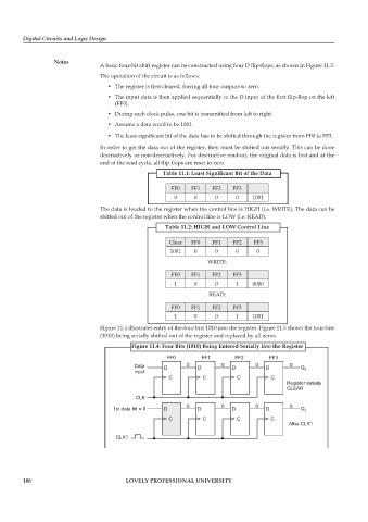
                                 A basic four-bit shift register can be constructed using four D flip-flops, as shown in Figure 11.3.
                                   The operation of the circuit is as follows:

                                    •  The register is first cleared, forcing all four outputs to zero.
                                    •  The input data is then applied sequentially to the D input of the first flip-flop on the left
                                      (FF0).
                                    •  During each clock pulse, one bit is transmitted from left to right.
                                    •  Assume a data word to be 1001.

                                    •  The least significant bit of the data has to be shifted through the register from FF0 to FF3.
                                 In order to get the data out of the register, they must be shifted out serially. This can be done
                                 destructively or non-destructively. For destructive readout, the original data is lost and at the
                                 end of the read cycle, all flip-flops are reset to zero.
                                                      Table 11.1: Least Significant Bit of the Data

                                                        FF0    FF1    FF2   FF3
                                                         0      0      0     0     1001
                                 The data is loaded to the register when the control line is HIGH (i.e. WRITE). The data can be
                                 shifted out of the register when the control line is LOW (i.e. READ).
                                                      Table 11.2: HIGH and LOW Control Line

                                                        Clear  FF0    FF1   FF2    FF3
                                                        1001    0      0     0      0
                                                                    WRITE:

                                                        FF0    FF1    FF2   FF3
                                                         1      0      0     1     0000
                                                                     READ:

                                                        FF0    FF1    FF2   FF3
                                                         1      0      0     1     1001
                                 Figure 11.4 illustrates entry of the-four bits 1010 into the register. Figure 11.5 shows the four-bits
                                 (1010) being serially shifted out of the register and replaced by all zeros.
                                            Figure 11.4: Four Bits (1010) Being Entered Serially into the Register

                                                       FF0        FF1        FF2        FF3
                                            Data      D      0   D       0  D       0  D       0  Q
                                            input                                                   3
                                                        C          C          C          C
                                                                                              Register initially
                                                                                              CLEAR
                                             CLK
                                                             0           0          0          0
                                      1st data hit=0  D          D          D          D          Q 3
                                                        C          C          C          C
                                                                                              After CLK1

                                       CLK1


        186                               LOVELY PROFESSIONAL UNIVERSITY

