Page 193 - DCAP108_DIGITAL_CIRCUITS_AND_LOGIC_DESIGNS
P. 193
Digital Circuits and Logic Design


                   Notes         5-Bit Serial-In/Serial-Out Shift Registers
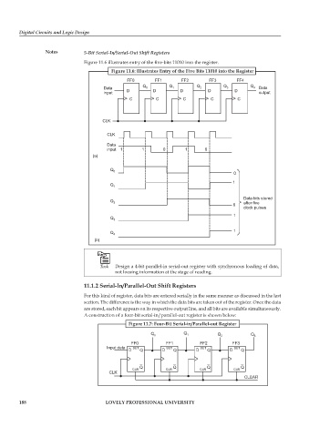
                                 Figure 11.6 illustrates entry of the five-bits 11010 into the register.
                                            Figure 11.6: Illustrates Entry of the Five Bits 11010 into the Register

                                                  FF0        FF1       FF2        FF3       FF4
                                                        Q         Q          Q         Q          Q
                                         Data            0         1          2         3          4 Data
                                         input    D         D         D          D         D         output
                                                   C         C          C         C          C


                                         CLK

                                          CLK
                                          Data
                                          input  1      1       0       1       0
                                     (a)

                                            Q 0
                                                                                           0

                                                                                           1
                                            Q 1
                                                                                               Data bits stored
                                            Q 2
                                                                                           0   after five
                                                                                               clock pulses
                                                                                           1
                                            Q 3

                                                                                           1
                                            Q 4
                                     (b)


                                             Design a 4-bit parallel-in serial-out register with synchronous loading of data,
                                             not loosing information at the stage of reading.

                                 11.1.2 Serial-In/Parallel-Out Shift Registers
                                 For this kind of register, data bits are entered serially in the same manner as discussed in the last
                                 section. The difference is the way in which the data bits are taken out of the register. Once the data
                                 are stored, each bit appears on its respective output line, and all bits are available simultaneously.
                                 A construction of a four-bit serial-in/parallel-out register is shown below:
                                                   Figure 11.7: Four-Bit Serial-in/Parallel-out Register


        188                               LOVELY PROFESSIONAL UNIVERSITY

