Page 197 - DCAP108_DIGITAL_CIRCUITS_AND_LOGIC_DESIGNS
P. 197
Digital Circuits and Logic Design


                   Notes
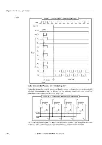
                                                    Figure 11.12: The Timing Diagram of 74HC165

                                          CLK
                                       CLK INH


                                          SER 0   (LOW)
                                                     1
                                         SHILD

                                            D 0

                                             D 1     0

                                             D 2     1

                                            D 3      0
                                      Data
                                             D 4     1

                                             D       0
                                              5
                                                     1
                                             D 6
                                             D 7     1

                                             Q 7                 1    1   0    1    0   1    0    1

                                             Q 7                 0    0   1    0    1   0    1    0


                                                       Inhibit                  Serial shift
                                                  Load
                                 11.1.5 Parallel-In/Parallel-Out Shift Registers

                                 For parallel-in/parallel-out shift registers, all data bits appear on the parallel outputs immediately
                                 following the simultaneous entry of the data bits. The following circuit is a four-bit parallel-in/
                                 parallel-out shift register constructed by D flip-flops.
                                                   Figure 11.13: Parallel-in/Parallel-out Shift Register

                                                 D 0           D 1           D 2           D 3

                                                    SET           SET           SET           SET
                                                  D    Q        D    Q        D    Q        D    Q


                                                       Q             Q             Q             Q
                                                    CLR           CLR           CLR           CLR
                                          CLEAR

                                           CLK
                                                         Q 0          Q 1           Q 2           Q 3
                                 The D’s are the parallel inputs and the Q’s are the parallel outputs. Once the register is clocked,
                                 all the data at the D inputs appear at the corresponding Q outputs simultaneously.


        192                               LOVELY PROFESSIONAL UNIVERSITY

