Page 13 - DCAP210_INTRODUCTION__TO_MICROPROCESSORS
P. 13
Unit 1: Microprocessors and Microcomputers


                                                                                                  Notes
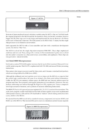
                                          Figure 1.7: MCS-4


            Busicom of Japan produced several calculator models using the MCS-4 chip set. Ted Hoff made
            the original proposal for the MCS-4 and did the feasibility study for the first calculator. Federico
            Faggin did all of the logic and circuit design and implemented the layout; Busicom’s M. Shima
            wrote most of Busicom’s firmware. The Intel patent on the MCS-4 has 17 claims, but the single
            chip processor is not claimed as an invention.
            Intel supported the MCS-4 with a Cross assembler and later with a standalone development
            system, the Intellec “blue” box.
            The MCS-4 evolved into the single chip microcomputers 8048/8051. These chips emphasized
            small size and low cost. These, along with a variety of other manufacturer’s parts, have evolved
            into the under 1 computer on a chip used in toys, automobiles, and appliances. These chips are
            very pervasive—almost invisible.

            1.2.3 Intel 8008 Microprocessor
            Intel made a custom 512-b shift register memory chip for use in (their customer) Data point’s low
            cost bit-serial computer. This 8-b CPU, implemented with TTL MSI, had around 50 data processing
            instructions.
            This custom chip design was never used by Data point, and it became a standard Intel product,
            which marketing dubbed the 8008 (twice 4004!).
            Although the arithmetic unit and registers were twice as large as in the MCS-4, we expected that
            the control logic could be about the same if we deleted a few Data point defined instructions.
            Unlike the MCS-4’s two-memory address space, the 8008 had one memory address space for
            program and data. The symmetric and regular instruction set was attractive. However, the only
            memory addressing was indirect through the High-Low (HL) register pair. Today’s computers
            have huge amounts of memory, and a plethora of memory addressing instructions.
            The 8008 CPU had six 8-b general purpose registers (B, C, D, E, H, L) and an 8-b accumulator. The
            push down program counter stack had 8-levels. Both of these register arrays were implemented
            with dynamic memory cells and the CPU had built-in “hidden” refresh during instruction fetch
            cycles, similar to the MCS-4.
            We decided that the 8008 would utilize standard memory components (not custom ROM’s and
            RAM’s as in the MCS-4). This increased the parts count on a minimum system because separate


                                     Figure 1.8: 8008 Microprocessor


                                             LOVELY PROFESSIONAL UNIVERSITY                                     7

