Page 140 - DCAP108_DIGITAL_CIRCUITS_AND_LOGIC_DESIGNS
P. 140
Unit 8: Memory


            array followed by a programmable OR gate array. To synthesize the output logic functions, first   Notes
            of all these are needed to be reduced to their minimum sum of product expressions. In PLA
            implementation, a designer should try to deduce these expressions in such a way that maximum
            number of common product terms exist between them. All these product terms are then generated
            in the AND gate array. From there, these product terms are fed in to the OR gate array where
            they are added according to the deduced logic expressions in order to get the output functions.

            The size of a programmable logic array is defined in terms of, number of inputs, number of product
            terms number of outputs etc. A, 4 input, 8, product terms and 4, output PLA will be defined as a
            (4, 8, 4) PLA. As the logic functions are synthesized almost in terms of their minimum sum of
            product expressions, the digital hardware required in a PLA is much less than that of a PROM.
            Also the costly decoder circuitry present in a PROM is replaced in the PLA by a more economical
            AND gate array. Use of less hardware also provides advantages in terms of speed, power
            consumptions, etc.

            The biggest disadvantage of a Programmable Logic Array is the two steps, programming involved.
            A designer has to first of all program the AND gate array and then program the OR gate array
            according to the programming of the AND gate array. Also PLA implementation requires the
            designer to try and deduce logic expressions with as many common terms between different
            expressions as possible. As this is an intuitive skill rather than a set procedure, that makes it very
            hard to automate or computerize the design process.
            To counter this problem, another line of programmable logic devices, known as PAL’s have
            been devised. These involve only one step programming while also it having similar hardware
            advantages of a PLA. In fact, PAL’s (programmable array logic) have become the most popular
            LSI programmable logic devices today, far surpassing PROM’s and PLA’s.
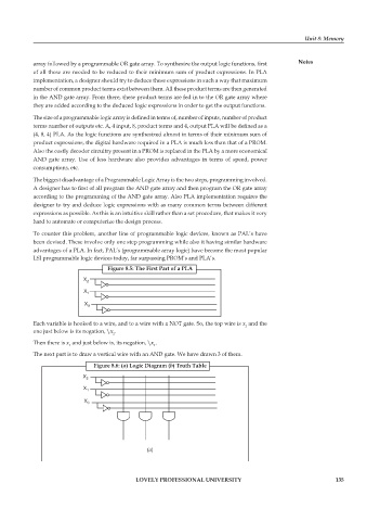
                                    Figure 8.5: The First Part of a PLA


            Each variable is hooked to a wire, and to a wire with a NOT gate. So, the top wire is x  and the
                                                                                 2
            one just below is its negation, \x .
                                      2
            Then there is x  and just below is, its negation, \x . 1
                       1
            The next part is to draw a vertical wire with an AND gate. We have drawn 3 of them.
                               Figure 8.6: (a) Logic Diagram (b) Truth Table


                                                 (a)


                                             LOVELY PROFESSIONAL UNIVERSITY                                   135

