Page 141 - DCAP108_DIGITAL_CIRCUITS_AND_LOGIC_DESIGNS
P. 141
Digital Circuits and Logic Design


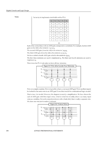
                   Notes                 Let us try to implement a truth table with a PLA.

                                                              x   x    x   z    z
                                                              2    1    0   1    0
                                                              0   0    0   0    0
                                                              0   0    1   1    0
                                                              0   1    0   0    0
                                                              0   1    1   1    0
                                                              1   0    0   1    1
                                                              1   0    1   0    0
                                                              1   1    0   0    0
                                                              1   1    1   0    1
                                                                      (b)
                                 Each of the vertical lines with an AND gate corresponds to a minterm. For example, the first AND
                                 gate (on the left) is the minterm: \x \x x .
                                                             2  1  0
                                 The second AND gate (from the left) is the minterm: \x x x .
                                                                             2 1 0
                                 The third AND gate (from the left) is the minterm: x \x \x .
                                                                             1
                                                                                0
                                                                           2
                                 We have added a fourth AND gate which is the minterm: x x x .
                                                                                2 1 0
                                 The first three minterms are used to implement z . The third and fourth minterms are used to
                                                                         1
                                 implement z .
                                           0
                                 This is how the PLA looks after we have all four minterms.
                                                     Figure 8.7: PLA After Loooks Four Minterms


                                 Now, you might complain. How is it possible to have a one input AND gate? How can three inputs
                                 be hooked to the same wire to an AND gate? Is not that invalid for combinational logic circuits?
                                 That is true, it is invalid. However, the diagram is merely a simplification. We have drawn the
                                 each of AND gate with three input wires, which is what it is in reality (there is as many input
                                 wires as variables). For each connection (shown with a black dot), there’s really a separate wire.
                                 We draw one wire just to make it look neat.
                                                             Figure 8.8: Vertical Wires


        136                               LOVELY PROFESSIONAL UNIVERSITY

