Page 86 - DCAP210_INTRODUCTION__TO_MICROPROCESSORS
P. 86

Introduction to Microprocessors


                  Notes          INTA (Pin 11)

                                 It stands for interrupt acknowledge. A low on this pin indicates that the microprocessor has
                                 acknowledged a request from some of the peripheral devices and is also used to activate the
                                 interrupt controller.
                                 Multiplexed Address/Data bus (Pin 12 to Pin 19)
                                 The pins 12 to 19 serve the dual purpose of transmitting the lower order address and data type is
                                 time division multiplexing. During the 1  clock of each machine cycle, the lower order address
                                                                  st
                                 byte is output on these lines. In the remaining part of the clock of the machine cycle, it becomes
                                 the data bus. The lower order address and data bus can be separated using an address latch.
                                 These are bidirectional bus. (AD  – AD )
                                                           0    7
                                 Latch
                                 It is commonly used to connect the output devices to the microprocessor. The data is available on
                                 the address/data bus for only a few microseconds. The data in the form of address must be
                                 present on the address bus so long as the reading or writing operation is not complete or otherwise
                                                                                                      st
                                 wrong data transfer will take place. Since the lower order address byte is present in the 1 clock of
                                 the machine cycle, it must be latched (stored to hold the lower order address byte). V  (Pin 20) is
                                                                                                    ss
                                 used for ground references.
                                 Address Bus (Pin 21 to Pin 28)
                                 8085A has eight unidirectional (A  to A ) signal lines corresponding to; pin 21 to pin 28. It outputs
                                                            8   15
                                 8-MSB’s (Most Significant Bit) i.e., higher order address bus of the memory address. It remains in
                                 the high impedance state during HOLD, HALT and RESET modes.
                                 Control and Status Signals

                                  RD  and  WR  are two control signals and 10/M,  S  and S  are the three status signals. The ALE is
                                                                         l    o
                                 a very special control signal, which indicates the beginning of the operation.
                                 S  (Pin 33) and S  (Pin 29)
                                  1            o
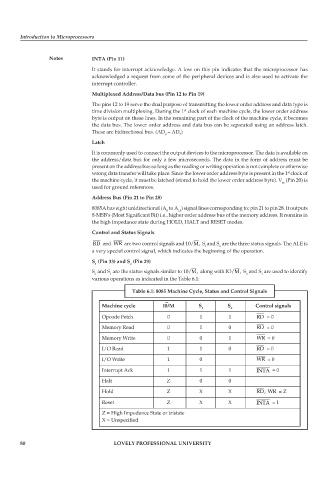
                                 S  and S  are the status signals similar to 10/M,  along with IO/M,  S  and S  are used to identify
                                  o     1                                               o    1
                                 various operations as indicated in the Table 6.1:
                                                Table 6.1: 8085 Machine Cycle, Status and Control Signals

                                                           –
                                     Machine cycle        I0/M         S         S         Control signals
                                                                        1         0
                                     Opcode Fetch           0          1         1         RD  = 0
                                     Memory Read            0          1         0         RD  = 0

                                     Memory Write           0          0         1         WR  = 0
                                     I/O Read               1          1         0         RD  = 0
                                     I/O Write              1          0                   WR  = 0

                                     Interrupt Ack          1          1         1         INTA  = 0
                                     Halt                   Z          0         0
                                     Hold                   Z          X         X         RD,  WR  = Z

                                     Reset                  Z          X         X         INTA  = 1
                                     Z = High Impedance State or tristate
                                     X = Unspecified


        80                               LOVELY PROFESSIONAL UNIVERSITY
   81   82   83   84   85   86   87   88   89   90   91