Page 88 - DCAP210_INTRODUCTION__TO_MICROPROCESSORS
P. 88
Introduction to Microprocessors


                                                                                      st
                  Notes                         The lower order address byte is present in the 1 clock of the machine cycle; it
                                                must be latched (stored to hold the lower order address byte). V  (Pin 20) is
                                                                                                    ss
                                                used for ground references.
                                 V  (Pin 40)
                                   cc
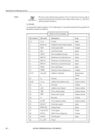
                                 An external DC supply voltage of +5V (17 milli-amps) is connected to this pin for the operation of
                                 the 8085A as shown in Table 6.2.

                                                             Table 6.2: Pin description

                                     Pin number   Pin name     Description                  Type

                                     1, 2         X , X        Crystal                      Input
                                                   1  2
                                     3            Reset out    Peripheral Reset Output Signal  Output

                                     4            SOD          Serial output data           Output
                                     5            SID          Serial Input data            Input

                                     6            TRAP         Non-maskable interrupt       Input
                                     7            RST 7.5      Hardware vectored interrupt  Input
                                     8            RST 6.5      Hardware vectored interrupt  Input

                                     9            RST 5.5      Hardware vectored interrupt  Input
                                     10           INTR         Interrupt Request            Input

                                     11            INTA        Interrupt Acknowledgement    Output
                                     12-19        AD -AD       Address/ Data Bus            Bidirectional,
                                                     0   7
                                                                                            tristate
                                     20           V            Ground                       Input
                                                   ss
                                     21-28        A -A         Address Bus (Higher byte)    Output, tristate
                                                    8  15
                                     29           S            Bus state                    Output
                                                   0
                                     30           ALE          Address Latch Signal         Output, tristate

                                     31            WR          Write control signal         Output, tristate
                                     32            RD          Read control signal          Output, tristate
                                     33           S            Bus state                    Output
                                                   1
                                     34           IO/M         I/O or memory status         Output, tristate
                                     35           READY        Wait state request           Input

                                     36           RESET IN     System Reset                 Input
                                     37           CLK (OUT)    Clock signal                 Outpu
                                     38           HLDA         Hold Acknowledgment          Output

                                     39           HOLD         Hold Request                 Input
                                     40           V (+5V)      Power
                                                   cc


        82                               LOVELY PROFESSIONAL UNIVERSITY

