Page 114 - DCAP108_DIGITAL_CIRCUITS_AND_LOGIC_DESIGNS
P. 114
Unit 7: Standard Integrated Circuits (ICs)


            One problem that DTL does not solve is its low speed, especially when the transistor is being   Notes
            turned off. Turning off a saturated transistor in a DTL gate requires it to first pass through the
            active region before going into cut-off. Cut-off, however, will not be reached until the stored charge
            in its base has been removed. The dissipation of the base charge takes time if there is no available
            path from the base to ground. This is why some DTL circuits have a base resistor that is tied to
            ground, but even this requires some trade-offs. Another problem with turning off the DTL output
            transistor is the fact that the effective capacitance of the output needs to charge up through Rc
            before the output voltage rises to the final logic ‘1’ level, which also consumes a relatively large
            amount of time. TTL, however, solves the speed problem of DTL elegantly.


                        Draw the circuit diagram of 3-input DTL using NOR gate.

            7.3 Transistor-Transistor Logic (TTL)


            Transistor-Transistor Logic, or TTL, refers to the technology for designing and fabricating digital
            integrated circuits that employ logic gates consisting primarily of bipolar transistors. It overcomes
            the main problem associated with DTL, i.e. lack of speed.

            The input to a TTL circuit is always through the emitter(s) of the input transistor, which exhibits
            a low input resistance. The base of the input transistor, on the other hand, is connected to the Vcc
            line, which causes the input transistor to pass a current of about 1.6 mA when the input voltage
            to the emitter(s) is logic ‘0’, i.e. near ground. Letting a TTL input ‘float’ (left unconnected) will
            usually make it go to logic ‘1’, but such a state is vulnerable to stray signals, which is why it is
            good practice to connect TTL inputs to Vcc using 1 kohm pull-up resistors.
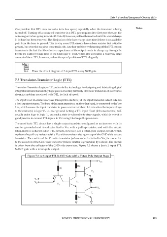
            The most basic TTL circuit has a single output transistor configured as an inverter with its
            emitter grounded and its collector tied to Vcc with a pull-up resistor, and with the output
            taken from its collector. Most TTL circuits, however, use a totem pole output circuit, which
            replaces the pull-up resistor with a Vcc-side transistor sitting on top of the GND-side output
            transistor. The emitter of the Vcc-side transistor (whose collector is tied to Vcc) is connected
            to the collector of the GND-side transistor (whose emitter is grounded) by a diode. The output
            is taken from the collector of the GND-side transistor. Figure 7.3 shows a basic 2-input TTL
            NAND gate with a totem-pole output.

                     Figure 7.3: A 2-input TTL NAND Gate with a Totem Pole Output Stage


                                             LOVELY PROFESSIONAL UNIVERSITY                                   109

