Page 118 - DCAP108_DIGITAL_CIRCUITS_AND_LOGIC_DESIGNS
P. 118
Unit 7: Standard Integrated Circuits (ICs)


            7.4.1 Implementation                                                                  Notes
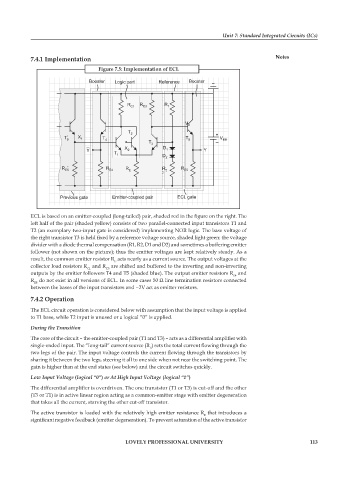
                                    Figure 7.5: Implementation of ECL


            ECL is based on an emitter-coupled (long-tailed) pair, shaded red in the figure on the right. The
            left half of the pair (shaded yellow) consists of two parallel-connected input transistors T1 and
            T2 (an exemplary two-input gate is considered) implementing NOR logic. The base voltage of
            the right transistor T3 is held fixed by a reference voltage source, shaded light green: the voltage
            divider with a diode thermal compensation (R1, R2, D1 and D2) and sometimes a buffering emitter
            follower (not shown on the picture); thus the emitter voltages are kept relatively steady. As a
            result, the common emitter resistor R  acts nearly as a current source. The output voltages at the
                                         E
            collector load resistors R  and R  are shifted and buffered to the inverting and non-inverting
                                C1
                                      C3
            outputs by the emitter followers T4 and T5 (shaded blue). The output emitter resistors R  and
                                                                                   E4
            R  do not exist in all versions of ECL. In some cases 50 Ω line termination resistors connected
             E5
            between the bases of the input transistors and −2V act as emitter resistors.
            7.4.2 Operation
            The ECL circuit operation is considered below with assumption that the input voltage is applied
            to T1 base, while T2 input is unused or a logical “0” is applied.
            During the Transition
            The core of the circuit – the emitter-coupled pair (T1 and T3) – acts as a differential amplifier with
            single-ended input. The “long-tail” current source (R ) sets the total current flowing through the
                                                      E
            two legs of the pair. The input voltage controls the current flowing through the transistors by
            sharing it between the two legs, steering it all to one side when not near the switching point. The
            gain is higher than at the end states (see below) and the circuit switches quickly.
            Low Input Voltage (logical “0”) or At High Input Voltage (logical “1”)
            The differential amplifier is overdriven. The one transistor (T1 or T3) is cut-off and the other
            (T3 or T1) is in active linear region acting as a common-emitter stage with emitter degeneration
            that takes all the current, starving the other cut-off transistor.

            The active transistor is loaded with the relatively high emitter resistance R  that introduces a
                                                                         E
            significant negative feedback (emitter degeneration). To prevent saturation of the active transistor


                                             LOVELY PROFESSIONAL UNIVERSITY                                   113

