Page 123 - DCAP108_DIGITAL_CIRCUITS_AND_LOGIC_DESIGNS
P. 123
Digital Circuits and Logic Design


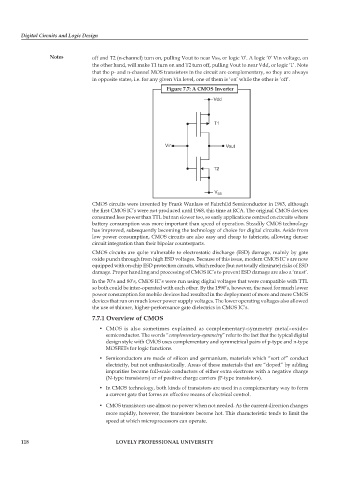
                   Notes         off and T2 (n-channel) turn on, pulling Vout to near Vss, or logic ‘0’. A logic ‘0’ Vin voltage, on
                                 the other hand, will make T1 turn on and T2 turn off, pulling Vout to near Vdd, or logic ‘1’. Note
                                 that the p- and n-channel MOS transistors in the circuit are complementary, so they are always
                                 in opposite states, i.e. for any given Vin level, one of them is ‘on’ while the other is ‘off’.
                                                            Figure 7.7: A CMOS Inverter


                                 CMOS circuits were invented by Frank Wanlass of Fairchild Semiconductor in 1963, although
                                 the first CMOS IC’s were not produced until 1968, this time at RCA. The original CMOS devices
                                 consumed less power than TTL but ran slower too, so early applications centred on circuits where
                                 battery consumption was more important than speed of operation. Steadily CMOS technology
                                 has improved, subsequently becoming the technology of choice for digital circuits. Aside from
                                 low power consumption, CMOS circuits are also easy and cheap to fabricate, allowing denser
                                 circuit integration than their bipolar counterparts.
                                 CMOS circuits are quite vulnerable to electrostatic discharge (ESD) damage, mainly by gate
                                 oxide punch through from high ESD voltages. Because of this issue, modern CMOS IC’s are now
                                 equipped with on-chip ESD protection circuits, which reduce (but not totally eliminate) risks of ESD
                                 damage. Proper handling and processing of CMOS IC’s to prevent ESD damage are also a ‘must’.
                                 In the 70’s and 80’s, CMOS IC’s were run using digital voltages that were compatible with TTL
                                 so both could be inter-operated with each other. By the 1990’s, however, the need for much lower
                                 power consumption for mobile devices had resulted in the deployment of more and more CMOS
                                 devices that run on much lower power supply voltages. The lower operating voltages also allowed
                                 the use of thinner, higher-performance gate dielectrics in CMOS IC’s.
                                 7.7.1 Overview of CMOS
                                    •  CMOS  is  also  sometimes  explained  as  complementary-symmetry  metal–oxide–
                                      semiconductor. The words “complementary-symmetry” refer to the fact that the typical digital
                                      design style with CMOS uses complementary and symmetrical pairs of p-type and n-type
                                      MOSFETs for logic functions.
                                    •  Semiconductors are made of silicon and germanium, materials which “sort of” conduct
                                      electricity, but not enthusiastically. Areas of these materials that are “doped” by adding
                                      impurities become full-scale conductors of either extra electrons with a negative charge
                                      (N-type transistors) or of positive charge carriers (P-type transistors).
                                    •  In CMOS technology, both kinds of transistors are used in a complementary way to form
                                      a current gate that forms an effective means of electrical control.
                                    •  CMOS transistors use almost no power when not needed. As the current direction changes
                                      more rapidly, however, the transistors become hot. This characteristic tends to limit the
                                      speed at which microprocessors can operate.


        118                               LOVELY PROFESSIONAL UNIVERSITY

