Page 125 - DCAP108_DIGITAL_CIRCUITS_AND_LOGIC_DESIGNS
P. 125
Digital Circuits and Logic Design


                   Notes
                                    Logic High Output Current, Ioh    mA   This is the maximum amount of current
                                                                           that an output of a CMOS digital IC can
                                                                           source while at Logic “1”.
                                                                           Example of an Actual Spec:
                                                                           –0.5 mA max. when Vss = 5V; Vin = 3.5V
                                    Logic Low Output Current, Iol     mA   This is the maximum amount of current
                                                                           that an output of a CMOS digital IC can
                                                                           sink while at Logic “0”.
                                                                           Example of an Actual Spec: +0.4 mA max.
                                                                           when Vss = 5V; Vin = 1.5V


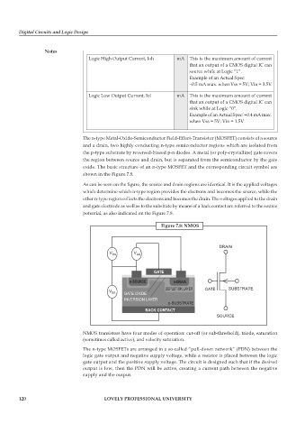
                                 The n-type Metal-Oxide-Semiconductor Field-Effect-Transistor (MOSFET) consists of a source
                                 and a drain, two highly conducting n-type semiconductor regions which are isolated from
                                 the p-type substrate by reversed-biased p-n diodes. A metal (or poly-crystalline) gate covers
                                 the region between source and drain, but is separated from the semiconductor by the gate
                                 oxide. The basic structure of an n-type MOSFET and the corresponding circuit symbol are
                                 shown in the Figure 7.8.
                                 As can be seen on the figure, the source and drain regions are identical. It is the applied voltages
                                 which determine which n-type region provides the electrons and becomes the source, while the
                                 other n-type region collects the electrons and becomes the drain. The voltages applied to the drain
                                 and gate electrode as well as to the substrate by means of a back contact are referred to the source
                                 potential, as also indicated on the Figure 7.8.

                                                                Figure 7.8: NMOS


                                                                                       DRAIN
                                            V        V
                                             DS       GS


                                                             GATE
                                                    n-SOURCE         n-DRAIN
                                                                  DEPLETION LAYER  GATE   SUBSTRATE
                                            V BS  GATE OXIDE
                                                 INVERSION LAYER
                                                                   p-SUBSTRATE
                                                          BACK CONTACT
                                                                                      SOURCE


                                 NMOS transistors have four modes of operation: cut-off (or sub-threshold), triode, saturation
                                 (sometimes called active), and velocity saturation.
                                 The n-type MOSFETs are arranged in a so-called “pull-down network” (PDN) between the
                                 logic gate output and negative supply voltage, while a resistor is placed between the logic
                                 gate output and the positive supply voltage. The circuit is designed such that if the desired
                                 output is low, then the PDN will be active, creating a current path between the negative
                                 supply and the output.


        120                               LOVELY PROFESSIONAL UNIVERSITY

