Page 244 - DCAP108_DIGITAL_CIRCUITS_AND_LOGIC_DESIGNS
P. 244
Unit 12: A/D and D/A Converters


                                                                                                  Notes
            Successive-approx imation register: When dealing with conversion times this short, it
            is usually necessary to take into account the other delays in the system (e.g., switching
            time of the multiplexer, settling time of the ladder network, comparator delay, and settling
            time).
            Free-running mode: All the logic blocks inside the dashed line in Figure 12.30a, or
            some equivalent arrangement, are frequently constructed on a single MSI chip; this
            chip is called a successive approximation register (SAR). For example, the Motorola
            MC6108 shown in Figure 12.30c is an 8-bit microprocessor-compatible A/D converter
            that includes an SAR, D/A conversion capabilities, control logic, and buffered digital
            outputs, in a 28-pin DIP.

            12.8.2 The ADC0804
            The ADC0804 is an inexpensive and very popular A/D converter which is available from
            a number of different manufacturers, including National Semiconductor. The ADC0804 is
            an 8-bit CMOS microprocessor-compatible successive-approximation A/D converter that is
            supplied in a 20-pin DIP. It is capable of digitizing an analog input voltage within the range
            0 to +5 Vdc, and it only requires a single dc supply voltage—usually +5 Vdc. The digital
            outputs are both TTL- and CMOS-compatible.

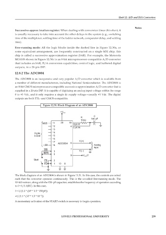
                                Figure 12.31: Block Diagram of an ADC0804


            The block diagram of an ADC0804 is shown in Figure 11.31. In this case, the controls are wired
            such that the converter operates continuously. This is the so-called free-running mode. The
            10–kW resistor, along with the 150–pF capacitor, establishes the frequency of operation according
            to f ≈ 1/1.1(RC). In this case,

            f ≈ 1/(1.1 * (10  * 1.5 * 150pF))
                       4
            =1/(1.1 * (10  * 1.5 * 10 ))
                              –12
                      4
            A momentary activation of the START switch is necessary to begin operation.


                                             LOVELY PROFESSIONAL UNIVERSITY                                   239

