Page 249 - DCAP108_DIGITAL_CIRCUITS_AND_LOGIC_DESIGNS
P. 249
Digital Circuits and Logic Design


                   Notes         advantage here is that the RC terms cancel from both sides of the equation above—in other
                                 words, this technique is free from the absolute values of either R or C and also from variations
                                 in either value.
                                 As a concrete example, let us suppose that the clock in Figure 12.34 is 1.0 MHz, the reference
                                 voltage is –1.0 Vdc, the fixed time period t1 is 1000 ms, and the RC time constant of the integrator
                                 is set at RC = 1.0 ms. During the time period t  the integrator voltage V  will ramp down to
                                                                                            c
                                                                       1
                                 –1.0 Vdc if V  = 1.0 V. Then, during, time t , V . will ramp all the way back up to 0.0 V, and this
                                            X
                                                                   2
                                                                      c
                                 will require a time of 1000 ms, since the slope of this ramp is fixed at 1.0 V/ms. The output display
                                 will now read 1000, and with placement of a decimal as shown, this reads 1.000 V.
                                 Another way of expressing the operation of this A/D converter is to solve the equation
                                 V  = V (t /t ) for t , since t  is the digital readout. Thus t  =(V /V )ti. If the same values as given
                                        2
                                           1
                                                                                     r
                                   X
                                                                                  X
                                       r
                                                      2
                                                2
                                                                              2
                                 above are applied, an unknown input voltage V  = 2.75 V will be digitized and the readout will be
                                                                       X
                                 t  = (2.7511.0)1000 = 2750, or 2.75 V, using the decimal point on the display. Notice that we have
                                  2
                                 used t  = 1000, the number of clock pulses that occur during the time period t . Likewise, t  is the
                                      1
                                                                                                        2
                                                                                              l
                                 number of clock pulses that occur during the time period t .
                                                                                2
                                                The analog signal is continuous in time and it is necessary to convert this to
                                                a flow of digital values.
                                 12.10 Single-Slope A/D Converter
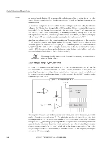
                                 In Figure 12.35, you can see a single-slope ADC. If you pay close attention, you will see that
                                 it is very similar to a ramp counter ADC, as it uses a counter, but instead of using a DAC for
                                 generating the comparison voltage, it uses a circuit called integrator, which is basically formed
                                 by a capacitor, a resistor and an operational amplifier (op amp). The MOSFET transistor makes
                                 the necessary control circuit.
                                                           Figure 12.35: Single-slope ADC


                                 The integrator produces a saw-tooth waveform on its output, from zero to the maximum possible
                                 analog voltage to be sampled, set by -V . The minute the waveform is started, the counter starts
                                                                ref
                                 counting from 0 to 2 – 1, where n is the number of bits implemented by the ADC. When the
                                                  n
                                 voltage found at   (the analog signal) is equal to the voltage achieved by the triangle waveform
                                               Vin
                                 generated by the integrator, the control circuit captures the last value produced by the counter
                                 (by trigging the output buffer clock pin), which will be the digital correspondent of the analog
                                 sample being converted. At the same time, it resets the counter and the integrator, starting the
                                 conversion of the next sample.


        244                               LOVELY PROFESSIONAL UNIVERSITY

