Page 253 - DCAP108_DIGITAL_CIRCUITS_AND_LOGIC_DESIGNS
P. 253
Digital Circuits and Logic Design


                   Notes
                                 12.13 Flash Converters


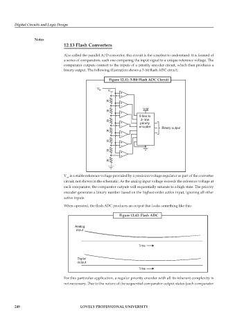
                                 Also called the parallel A/D converter, this circuit is the simplest to understand. It is formed of
                                 a series of comparators, each one comparing the input signal to a unique reference voltage. The
                                 comparator outputs connect to the inputs of a priority encoder circuit, which then produces a
                                 binary output. The following illustration shows a 3-bit flash ADC circuit:

                                                        Figure 12.41: 3-Bit Flash ADC Circuit


                                 V  is a stable reference voltage provided by a precision voltage regulator as part of the converter
                                   ref
                                 circuit, not shown in the schematic. As the analog input voltage exceeds the reference voltage at
                                 each comparator, the comparator outputs will sequentially saturate to a high state. The priority
                                 encoder generates a binary number based on the highest-order active input, ignoring all other
                                 active inputs.
                                 When operated, the flash ADC produces an output that looks something like this:

                                                             Figure 12.42: Flash ADC


                                 For this particular application, a regular priority encoder with all its inherent complexity is
                                 not necessary. Due to the nature of the sequential comparator output states (each comparator


        248                               LOVELY PROFESSIONAL UNIVERSITY

