Page 251 - DCAP108_DIGITAL_CIRCUITS_AND_LOGIC_DESIGNS
P. 251
Digital Circuits and Logic Design


                   Notes         12.12 Successive Approximation A/D Converter

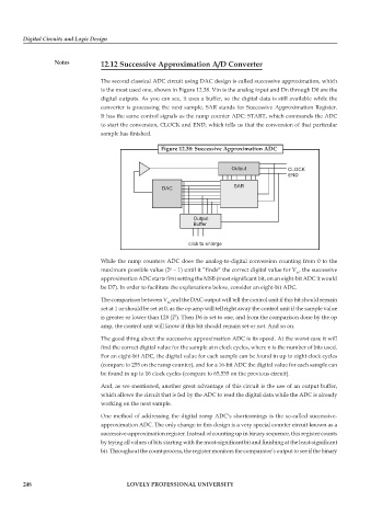
                                 The second classical ADC circuit using DAC design is called successive approximation, which
                                 is the most used one, shown in Figure 12.38. Vin is the analog input and Dn through D0 are the
                                 digital outputs. As you can see, it uses a buffer, so the digital data is still available while the
                                 converter is processing the next sample. SAR stands for Successive Approximation Register.
                                 It has the same control signals as the ramp counter ADC: START, which commands the ADC
                                 to start the conversion, CLOCK and END, which tells us that the conversion of that particular
                                 sample has finished.

                                                     Figure 12.38: Successive Approximation ADC


                                                                           Output            CLOCK
                                                                                             END
                                                     DAC                    SAR


                                                               Output
                                                               Buffer


                                                              click to enlarge

                                 While the ramp counters ADC does the analog-to-digital conversion counting from 0 to the
                                 maximum possible value (2  – 1) until it ”finds“ the correct digital value for V , the successive
                                                        n
                                                                                                in
                                 approximation ADC starts first setting the MSB (most significant bit, on an eight-bit ADC it would
                                 be D7). In order to facilitate the explanations below, consider an eight-bit ADC.
                                 The comparison between V  and the DAC output will tell the control unit if this bit should remain
                                                       in
                                 set at 1 or should be set at 0, as the op amp will tell right away the control unit if the sample value
                                 is greater or lower than 128 (2 ). Then D6 is set to one, and from the comparison done by the op
                                                         7
                                 amp, the control unit will know if this bit should remain set or not. And so on.
                                 The good thing about the successive approximation ADC is its speed. At the worst case it will
                                 find the correct digital value for the sample at n clock cycles, where n is the number of bits used.
                                 For an eight-bit ADC, the digital value for each sample can be found in up to eight clock cycles
                                 (compare to 255 on the ramp counter), and for a 16-bit ADC the digital value for each sample can
                                 be found in up to 16 clock cycles (compare to 65,535 on the previous circuit).
                                 And, as we mentioned, another great advantage of this circuit is the use of an output buffer,
                                 which allows the circuit that is fed by the ADC to read the digital data while the ADC is already
                                 working on the next sample.
                                 One method of addressing the digital ramp ADC’s shortcomings is the so-called successive-
                                 approximation ADC. The only change in this design is a very special counter circuit known as a
                                 successive-approximation register. Instead of counting up in binary sequence, this register counts
                                 by trying all values of bits starting with the most-significant bit and finishing at the least-significant
                                 bit. Throughout the count process, the register monitors the comparator’s output to see if the binary


        246                               LOVELY PROFESSIONAL UNIVERSITY

