Page 250 - DCAP108_DIGITAL_CIRCUITS_AND_LOGIC_DESIGNS
P. 250
Unit 12: A/D and D/A Converters


            Like the successive approximation ADC, this circuit uses an output buffer, meaning that the last   Notes
            converted value can be read while the ADC is converting the current value.
            Even though its design is simpler than ramp counter design, it is still based on a counter, and
            thus suffering from the same basic problem found on ramp counter design: speed. It requires
            up to 2  - 1 clock cycles to convert each sample. For an eight-bit ADC, it would take up to 255
                  n
            clock cycles to convert a single sample. For a 16-bit ADC it would take up to 65,535 clock cycles
            to convert one sample.

            12.11 Dual-slope A/D Converter

            Another popular design based on this one is called dual-slope ADC, which solves an inherent
            single-slop problem called calibration drift, which leads to inaccuracy over time because the
            integrator is not linked to the clock signal (i.e. the saw-tooth waveform is not synchronized with
            the counter clock).
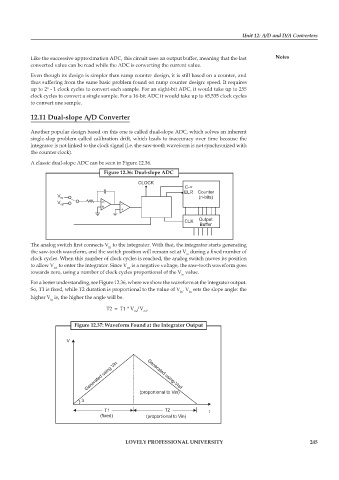
            A classic dual-slope ADC can be seen in Figure 12.36.
                                      Figure 12.36: Dual-slope ADC

                                                  CLOCK
                                                                  C-<
                                                                  ELR  Counter
                     V                                                 (n-bits)
                      in
                     V ref           –      –
                                     +
                                           +
                                                                       Output
                                                                  CLK
                                                                       Buffer

            The analog switch first connects V  to the integrator. With that, the integrator starts generating
                                       in
            the saw-tooth waveform, and the switch position will remain set at V  during a fixed number of
                                                                  in
            clock cycles. When this number of clock cycles is reached, the analog switch moves its position
            to allow V  to enter the integrator. Since V  is a negative voltage, the saw-tooth waveform goes
                                              ref
                    ref
            towards zero, using a number of clock cycles proportional of the V  value.
                                                                 in
            For a better understanding, see Figure 12.36, where we show the waveform at the integrator output.
            So, T1 is fixed, while T2 duration is proportional to the value of V . V  sets the slope angle: the
                                                                in  in
            higher V  is, the higher the angle will be.
                   in
                                      T2  =  T1 * V /V .
                                                in  ref
                           Figure 12.37: Waveform Found at the Integrator Output


                                             LOVELY PROFESSIONAL UNIVERSITY                                   245

