Page 96 - DCAP108_DIGITAL_CIRCUITS_AND_LOGIC_DESIGNS
P. 96
Unit 6: Implementation of Combinational Logic Circuit


            This general design procedure has five main steps. First, you must gain a clear understanding of   Notes
            the design intent of each circuit before any design activities start. When you are doing original
            design work, this understanding comes from many sources, including other persons, previous
            or competing designs, research papers, or your own insightful thinking. For now, the discussion
            that leads the presentation of each new circuit is intended to impart that clear understanding to
            you. Second, a block diagram that shows all circuit inputs and outputs will be developed. A block
            diagram is an indispensable part of any design, especially when dealing with complex circuits.
            In conceiving and capturing a block diagram, you are committing to a set of input and output
            signals, and those signals define the context and boundaries of your design. Third, the design
            requirements will be captured in an engineering formalism like a truth table or logic equation.
            This formalism removes all ambiguity from the design, and establishes a solid specification for
            the circuit. Fourth, the formally stated requirements will be used to find minimal circuits that
            meet the specifications. And finally, those minimal circuits will be created and implemented
            using the ISE/WebPack tool and a Digilent board, and verified in hardware to ensure they meet
            their behavioural requirements. In practice, a few types of logic circuits are often used as building
            blocks in larger designs.

            6.1 Multiplexers


            A multiplexer circuit has a number of data inputs, one or more select inputs, and one output.
            It passes the signal value on one of the data inputs to the output. The data input is selected by
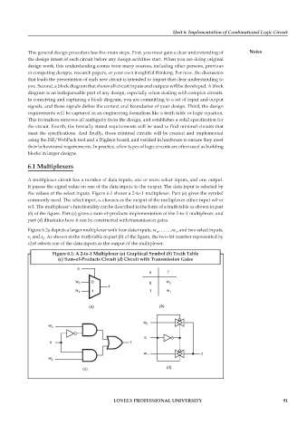
            the values of the select inputs. Figure 6.1 shows a 2-to-1 multiplexer. Part (a) gives the symbol
            commonly used. The select input, s, chooses as the output of the multiplexer either input w0 or
            w1. The multiplexer’s functionality can be described in the form of a truth table as shown in part
            (b) of the figure. Part (c) gives a sum-of-products implementation of the 2-to-1 multiplexer, and
            part (d) illustrates how it can be constructed with transmission gates.

            Figure 6.2a depicts a larger multiplexer with four data inputs, w ,……..,w , and two select inputs,
                                                              0
                                                                     3
            s  and s . As shown in the truth table in part (b) of the figure, the two-bit number represented by
                  0
             1
            s1s0 selects one of the data inputs as the output of the multiplexer.
                     Figure 6.1: A 2-to-1 Multiplexer (a) Graphical Symbol (b) Truth Table
                        (c) Sum-of-Products Circuit (d) Circuit with Transmission Gates
                               s
                                                           s      f
                              w 0    0                     0      w 0
                                           f
                              w      1                     1      w
                               1                                   1

                                                               b
                                    a
                                   ()                          ()
                                                         w
                    w 0                                   0
                                                         s
                    s                               f

                                                         w 1                   f
                    w 1
                                                                  d
                                  c
                                 ()                               ()


                                             LOVELY PROFESSIONAL UNIVERSITY                                    91

