Page 98 - DCAP210_INTRODUCTION__TO_MICROPROCESSORS
P. 98
Introduction to Microprocessors


                  Notes          current instruction, while the address used in the Memory read cycle can, have several possible
                                 origins. The data read during memory read cycle is placed in the appropriate register and not in
                                 the instruction register.

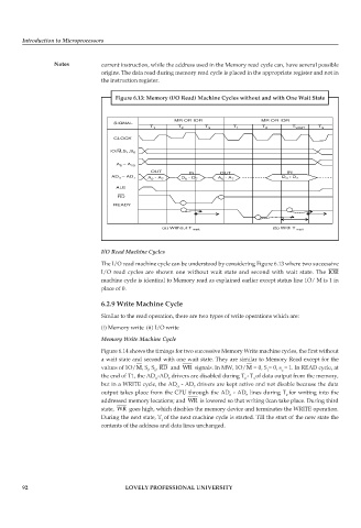
                                      Figure 6.13: Memory (I/O Read) Machine Cycles without and with One Wait State


                                 I/O Read Machine Cycles
                                 The I/O read machine cycle can be understood by considering Figure 6.13 where two successive
                                 I/O read cycles are shown one without wait state and second with wait state. The  IOR
                                 machine cycle is identical to Memory read as explained earlier except status line 1O/ M is 1 in
                                 place of 0.

                                 6.2.9 Write Machine Cycle
                                 Similar to the read operation, there are two types of write operations which are:

                                 (i) Memory write (ii) I/O write
                                 Memory Write Machine Cycle

                                 Figure 6.14 shows the timings for two successive Memory Write machine cycles, the first without
                                 a wait state and second with one wait state. They are similar to Memory Read except for the
                                 values of 1O/M, S , S , RD  and  WR  signals. In MW, 1O/M = 0, S = 0, s = 1. In READ cycle, at
                                                l  0                                  1    o
                                 the end of T1, the AD -AD  drivers are disabled during T - T of data output from the memory,
                                                   O   7                       2     3
                                 but in a WRITE cycle, the AD  - AD  drivers are kept active and not disable because the data
                                                          O    7
                                 output takes place from the CPU through the AD  - AD  lines during T for writing into the
                                                                          0     7           2
                                 addressed memory locations; and  WR  is lowered so that writing 0can take place. During third
                                 state,  WR  goes high, which disables the memory device and terminates the WRITE operation.
                                 During the next state, T of the next machine cycle is started. Till the start of the new state the
                                                     1
                                 contents of the address and data lines unchanged.


        92                               LOVELY PROFESSIONAL UNIVERSITY

