Page 96 - DCAP210_INTRODUCTION__TO_MICROPROCESSORS
P. 96
Introduction to Microprocessors


                  Notes          The instruction fetch timing diagram can be in various steps.

                                 •  Initially the 10/ M are low and S are S are high to indicate the opcode fetch operation. In this
                                                              o   1
                                    state ALE is high and PC’s higher byte is placed on the A  A  address lines and lower byte is
                                                                                 8  15
                                    placed on to A  -A by dimultiplexing AD lines.
                                                0  7
                                 •  In the second state the CPU sends low on RD pin by which MEMRD signal is generated for
                                    read operation.
                                 •  In third state the opcode is read from memory location addressed by program counter. The
                                    read signal is high at the end of this cycle.
                                 •  In fourth state the opcode is decoded and is ready to receive next instruction or machine
                                    cycle.

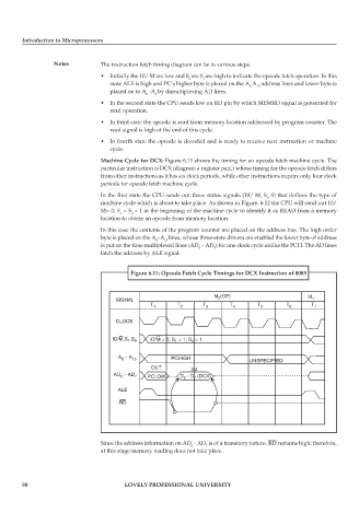
                                 Machine Cycle for DCX: Figure 6.11 shows the timing for an opcode fetch machine cycle. The
                                 particular instruction is DCX (diagram a register pair,) whose timing for the opcode fetch differs
                                 from other instructions as it has six clock periods, while other instructions require only four clock
                                 periods for opcode fetch machine cycle.

                                 In the first state the CPU sends out three status signals (10/ M, S , S) that defines the type of
                                                                                       o
                                 machine cycle which is about to take place. As shown in Figure. 6.12 the CPU will send out 10/
                                 M= 0; S  = S = 1 at the beginning of the machine cycle to identify it as READ from a memory
                                        1  o
                                 location to obtain an opcode from memory location.
                                 In this case the contents of the program counter are placed on the address bus. The high order
                                 byte is placed on the A -A lines, whose three-state drivers are enabled the lower byte of address
                                                   8    15
                                 is put on the time multiplexed lines (AD  – AD ) for one clock cycle unlike the PCH. The AD lines
                                                                 0    7
                                 latch the address by ALE signal.

                                           Figure 6.11: Opcode Fetch Cycle Timings for DCX Instruction of 8085


                                 Since the address information on AD  - AD  is of a transitory nature. RD remains high; therefore,
                                                              0    7
                                 at this stage memory reading does not take place.


        90                               LOVELY PROFESSIONAL UNIVERSITY

