Page 97 - DCAP210_INTRODUCTION__TO_MICROPROCESSORS
P. 97
Unit 6: The 8085 Microprocessor Architecture


                                                                                                  Notes
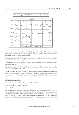
                        Figure 6.12: Opcode Fetch Machine Cycle with One wait State


            In the second state the lower address byte (PCL) disappears from AD -AD  lines. However, A A
                                                                  0   7              0   7
            information remains available. Now RD signal from CPU goes low which enables memory devices
            and opcode for DCX is put on to the data lines.

            During third state the CPU loads opcode into instruction register and RD signal is made, high
            which disables addressed memory device.

            During fourth state (T ), the opcode -is decoded by the instruction decoder and enters into the
                              4
            fifth state in this case.
            During fifth and sixth states (T  and T )CPU determines register and decrements it which internally
                                   5    6
            transfers to INC/DCR circuit of CPU.
            Opcode fetch with wait state: When extra time is required to fetch opcode from slow memory
            devices, the CPU should get READY signal low while checking it in second state (T). It introduces
            one wait cycle between T and T .When it receives it high on READY then only it proceeds to the
                                2    3
            next state.

            6.2.8 Read Cycle of 8085
            There are two types of read operations associated with this micro-processor

            (i) Memory Read, (ii) I/O Read operation
            Memory Read Cycle
            We can consider two successive memories read machine cycles which are shown in Figure 6.13
            without T   state and second with one T   state. The timing during T  - T  is absolutely identical
                    wait                    Wait                   l  3
            to the Opcode Fetch (OF) machine cycle, with the exception that the status sent out during T  is
                                                                                     1
            IO/ M= 0; S  =1; S  = 0, identifying the cycles as a READ from a memory location. The memory
                     1    o
            address used in OF cycle is always the contents of the program counter, which points to the


                                             LOVELY PROFESSIONAL UNIVERSITY                                    91

