Page 104 - DCAP108_DIGITAL_CIRCUITS_AND_LOGIC_DESIGNS
P. 104
Unit 6: Implementation of Combinational Logic Circuit


                                                                                                  Notes
                  Example: Here is an abbreviated truth table for the demultiplexer. We could have given

            the full table since it has only 16 rows, but we will use the same convention as for the multiplexer
            where we abbreviated the values of the data inputs.

                                    a2 a1 a0  d | x7 x6 x5 x4 x3 x2 x1 x0

                                       0  0  0  c |  0  0  0  0  0  0  0  c
                                       0  0  1  c |  0  0  0  0  0  0  c  0
                                       0  1  0  c |  0  0  0  0  0  c  0  0
                                       0  1  1  c |  0  0  0  0  c  0  0  0
                                       1  0  0  c |  0  0  0  c  0  0  0  0
                                       1  0  1  c |  0  0  c  0  0  0  0  0
                                       1  1  0  c |  0  c  0  0  0  0  0  0
                                       1  1  1  c |  c  0  0  0  0  0  0  0
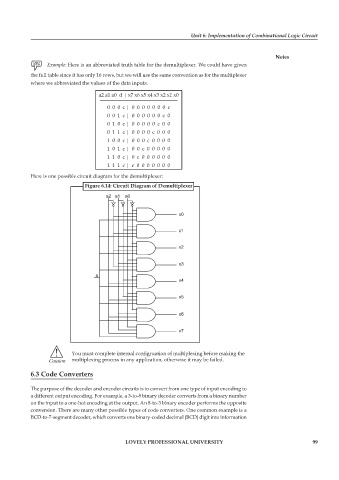
            Here is one possible circuit diagram for the demultiplexer:
                               Figure 6.14: Circuit Diagram of Demultiplexer


                          You must complete internal configruation of multiplexing before making the
                          multiplexing process in any application, otherwise it may be failed.

            6.3 Code Converters

            The purpose of the decoder and encoder circuits is to convert from one type of input encoding to
            a different output encoding. For example, a 3-to-8 binary decoder converts from a binary number
            on the input to a one-hot encoding at the output. An 8-to-3 binary encoder performs the opposite
            conversion. There are many other possible types of code converters. One common example is a
            BCD-to-7-segment decoder, which converts one binary-coded decimal (BCD) digit into information


                                             LOVELY PROFESSIONAL UNIVERSITY                                    99

