Page 102 - DCAP108_DIGITAL_CIRCUITS_AND_LOGIC_DESIGNS
P. 102
Unit 6: Implementation of Combinational Logic Circuit


            Self Assessment                                                                       Notes

            Choose the correct answer:
               1.  A device which converts BCD to Seven Segment is called:
                 (a)  Encoder                    (b)  Decoder
                 (c)  Multiplexer                (d)  Demultiplexer
               2.  The following switching functions are to be implemented using a Decoder:
                 f = Σm(1, 2, 4, 8, 10, 14), f = Σm(2, 5, 9, 11), f  = Σm(2, 4, 5, 6, 7)
                 1                   2              3
                 The minimum configuration of the decoder should be
                 (a)  2 – to – 4 line            (b)  3 – to – 8 line.
                 (c)  4 – to – 16 line           (d)  5 – to – 32 line.
               3.  Combinational circuit consists of input variables, logic gates and output variables.
                 (a)  True                       (b)  False

               4.  One multiplexer can take the place of:
                 (a)  several SSI logic gates
                 (b)  combinational logic circuits
                 (c)  several Ex-NOR gates
                 (d)  several SSI logic gates or combinational logic circuits

            6.2 Demultiplexer


            The demultiplexer is the inverse of the multiplexer, in that it takes a single data input and n
            address inputs. It has 2  outputs. The address input determine which data output is going to have
                              n
            the same value as the data input. The other data outputs will have the value 0.
            The data distributor, known more commonly as a Demultiplexer or “Demux”, is the exact opposite
            of the Multiplexer. The demultiplexer takes one single input data line and then switches it to any
            one of a number of individual output lines one at a time. The demultiplexer converts a serial data
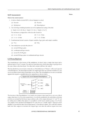
            signal at the input to a parallel data at its output lines as shown below:
                                 Figure 6.11: 1-to-4 Channel Demultiplexer


            The function of the Demultiplexer is to switch one common data input line to any one of the 4
            output data lines A to D in our example above. As with the multiplexer the individual solid state
            switches are selected by the binary input address code on the output select pins “a” and “b” and
            by adding more address line inputs it is possible to switch more outputs giving a 1-to-2  data
                                                                                   n
            line outputs. Some standard demultiplexer IC´s also have an “enable output” input pin which
            disables or prevents the input from being passed to the selected output. Also some have latches
            built into their outputs to maintain the output logic level after the address inputs have been


                                             LOVELY PROFESSIONAL UNIVERSITY                                    97

