Page 154 - DCAP108_DIGITAL_CIRCUITS_AND_LOGIC_DESIGNS
P. 154
Unit 9: Flip-Flops


            to the disc to generate timing pulses in response to the timing marks and supply the pulses to the   Notes
            shift register. Each of plural logic gates has two input terminals each of which is connected to an
            output of a predetermined step of the shift register, so that an output signal outputted from each
            logic gate to the corresponding driving circuit for an operating device constitutes timing signal
            carrying information including starting and terminating times of operation.

            9.1 Basic Flip-Flop Circuit

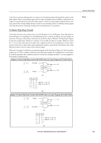
            A flip-flop circuit can be construct from two NAND gates or two NOR gates. These flip-flops are
            shown in Figure 9.1 and Figure 9.2. Each flip-flop has two outputs, Q and Q′, and two inputs, set
            and reset. This type of flip-flop is referred to as an SR flip-flop or SR latch. The flip-flop in Figure
            9.1 has two useful states. When Q = 1 and Q′ = 0, it is in the set state (or 1-state). When Q = 0 and
            Q′ = 1, it is in the clear state (or 0-state). The outputs Q and Q′ are complements of each other
            and are referred to as the normal and complement outputs, respectively. The binary state of the
            flip-flop is taken to be the value of the normal output.
            When an 1 is applied to both the set and reset inputs of the flip-flop in Figure 9.1, both Q and Q’
            outputs go to 0. This condition violates the fact that both outputs are complements of each other.
            In normal operations this condition must be avoided by making sure that 1’s are not applied to
            both inputs simultaneously.
               Figure 9.1: Basic Flip-Flop Circuit with NOR Gates (a) Logic Diagram (b) Truth Table

                             1        R (reset)
                                                                     Q


                                                                     Q
                             1         S (set)

                                                   a
                                                  ()
                                    SR    Q Q
                                    1 0   1 0
                                    0 0   1 0  (afterS=1,R=0)
                                    0 1   0 1  (afterS=0,R=1)
                                    0 0   0 1
                                    1 1   0 0
                                                   b
                                                  ()
              Figure 9.2: Basic Flip-Flop Circuit with NAND Gates (a) Logic Diagram (b) Truth Table

                             1
                                        S (set)                      Q


                                                                     Q
                             1         R (reset)

                                                    ()
                                                    a
                                           SR    QQ
                                           1 0   0 1
                                           1 1   0 1  (afterS=1,R=0)
                                           0 1   1 0  (afterS=0,R=1)
                                           1 1   1 0
                                           0 0   1 1
                                                    ()
                                                    b

                                             LOVELY PROFESSIONAL UNIVERSITY                                   149

