Page 157 - DCAP108_DIGITAL_CIRCUITS_AND_LOGIC_DESIGNS
P. 157
Digital Circuits and Logic Design


                   Notes
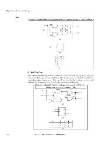
                                   Figure 9.5: Clocked T Flip-Flop (a) Logic Diagram (b) Graphical Symbol (c) Transition Table


                                                    T
                                                                                          Q
                                                   CP

                                                                                          Q


                                                                     ()
                                                                      a

                                                                   T    Q
                                                          CP
                                                                        Q

                                                                      b
                                                                     ()
                                                                 Q  J  Q(t+1)
                                                                 0  0   0
                                                                 0  1   1
                                                                 1  0   1
                                                                 1  1   0
                                                                    ()
                                                                     c
                                 9.2.4 D Flip-Flop

                                 The D flip-flop shown in Figure 9.6 is a modification of the clocked SR flip-flop. The D input goes
                                 directly into the S input and the complement of the D input goes to the R input. The D input is
                                 sampled during the occurrence of a clock pulse. If it is 1, the flip-flop is switched to the set state
                                 (unless it was already set). If it is 0, the flip-flop switches to the clear state.
                                           Figure 9.6: Clocked D Flip-Flop (a) Logic Diagram with NAND Gates
                                                      (b) Graphical Symbol (c) Transition Table

                                                 D
                                                                                             Q
                                                CP

                                                                                             Q

                                                                         ()
                                                                         a

                                                                      D   Q
                                                             CP
                                                                           Q
                                                                         b
                                                                         ()
                                                              D       Q        Q′
                                                              1        X        1
                                                              0        X        0
                                                                        (c)


        152                               LOVELY PROFESSIONAL UNIVERSITY

